|
|
Login to enhance your online experience. Login or Create an Account |
|
|
Categories
Main Menu
Shopping Cart
There are no items in your shopping cart. |
'ArsRegRw' - CPU registers and device hardware read/write Android appWARNING:The here presented utility is extremely powerful. You, as a user have to know exactly what are you doing while using it. By downloading and using the 'ArsRegRw' software package you release us from any responsibility. I. IntroYour Android device - a phone, a tablet, or any other type consists of a microprocessor (CPU), number of chips connected to it, and additional components - like a display, connectors, buttons, etc...From the point of view of the software, the CPU + device chips appear as a memory area which include individual and specific registers - residing within the 4gbytes memory space of a 32bit CPU. 'ArsRegRw' allows read/write of the CPU registers and the chips on device hardware app - almost all of the total 4gbytes space. II. Pre-requisites'ArsRegRw' is a software package consisting of :- 'ArsRegRw' Android app - software engine installed from the host side !!! If you didn't already do this, please go to - http://arstech.com/install/ecom-prodshow/arsregrw.html The page provides a download link to get the software engine and details on the installing and using. Pre-requisites to be able to use 'ArsRegRw' with an Android device are: 1. Allowed Root access '#' on the Android device; if the device does not have root access steps must be take to root it; if unable to root the device you will not be able to use 'ArsRegRw'. In addition, a host desktop/notebook system running Windows has to have USB drivers to connect to the Android device and run the ADB utility. The USB drivers and utility are provided by Google, and we maybe able to provide them if needed as re-distributables. Linux, and Mac OS X have support USB support on user level, however the ADB utility has be able to 'talk' through the provided support. 2. User's Guide / Technical reference manual (UM/TRM) .pdf file for the CPU on which the the specific Android device is based. The document should include a memory map and addresses of the built in peripherals - gpio, timers, i2c, spi, sdio/mmc, usb ... The list of CPU vendors include - Samsung, NVIDIA, Qualcomm, TI, Rockchip (China), Spreadtrum (China) ... Some of the vendors provide freely this info, and some under lots of conditions - which an individual software developer may or may not be able to meet. If unable to obtain directly info on the CPU, one indirect way is to comb the Linux kernel sources for registers and info on peripherals for a specific CPU. In addition, if possible to obtain, the schematic of a device will show which chips are connected to the CPU. Having UM/TRM for these chips will allow to use 'ArsRegRw' to access these chips as well. III. Installing and usingA host desktop/notebook system running Windows, or Linux, or Mac OS X is required to connect to the Android device. Go to -http://arstech.com/install/ecom-prodshow/arsregrw.html The page provides a download link to get the software engine and details on the installing and using. - download the installation software, unzip; under windows, if not already done - install USB driver for android device; - connect Android device, and install based on host OS - Win/Lin/Mac if not already done - install the ArsCmd.apk, and run 'arsregrw-andr' software engine; there are scripts provided - 'lnx/win-run-sw.bat' , and 'lnx/win-instal-app.bat' . Note: under Linux, you may need to make the scripts executable - chmod +x lnx-run-sw.bat chmod +x lnx-instal-app.bat The 'ArsRegRw' all has a field to enter a command, a command button, and a status field. Each command is a text string with 2 or 3 fields separated by space - a bbbbbbbb cccccccc , where - a) command - r=read memory, w=write memory bbbbbbbb) address - 32bit physical memory address dddddddd) data - 32bit data (to write, not used in read) Note: normally hardware (CPU, peripherals) is accessed through a device driver (kernel module); a driver can not use directly a physical address; it has to obtain a virtual address for the specific physical address; 'ArsRegRw' allows using directly the physical address; Examples: r 10ab00f0 - 32bit read from physical memory address 0x10ab00f0 w 2CE0A000 FFFF0000 - 32bit write of 0xFFFF0000 to physical memory address 0x2CE0A000 IV. TutorialWe did test 'ArsRegRw' app on 2 boards:- pandaboard - based on TI OMAP4 processor - origen - based on Samsung Exynos 4 processor The deices were set to boot Android, and already had root access allowed. The location of the UM/TRM documents are: - ti.com - omap4770 tech.ref.man. .pdf 5807 pages - samsung.com - exynos4 quad (exynos 4412) .pdf 913 pages 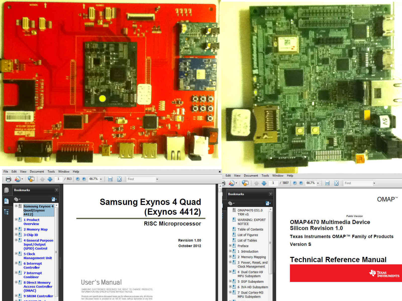 origen board, pandaboard, and UM/TRM origen board, pandaboard, and UM/TRM We provide 3 exercises, with specific pointers. !!! IMPORTANT: Download the above 2 documents, and before doing the specific exercise - turn to the specific page , read and understand the information. Exercise1 *** chip id *** Each CPU vendor places information on the CPU id/number/revision on a specific memory location. Software can use this info to support a variety of options with a single program, and also to patch and fix things. - ti omap .pdf page 288, ch. 1.5 OMAP4470 Family and Device Identification STD_FUSE_DIE_ID_0[31:0] 0x4A00 2200 ID_CODE[31:0] 0x4A00 2204 STD_FUSE_DIE_ID_1[31:0] 0x4A00 2208 STD_FUSE_DIE_ID_2[31:0] 0x4A00 220C STD_FUSE_DIE_ID_3[31:0] 0x4A00 2210 STD_FUSE_PROD_ID_0[31:0] 0x4A00 2214 STD_FUSE_PROD_ID_1[31:0] 0x4A00 2218 Command : r 4A002200 - reads STD_FUSE_DIE_ID_0 - samsung exynos .pdf page37 , ch. 3.2.1.1 PRO_ID Base Address: 0x1000_0000 PRO_ID 0x0000 Product information (ID, package, and revision) 0xE441_2XXX PACKAGE_ID 0x0004 Package information (POP type and package) 0xXXXX_XXXX Command : r 10000000 - reads PRO_ID Exercise2 *** gpio *** Every ARM SOC CPU has a large number of gpio pins, which can be configured by software to connect to a function - i2c, timer, spi, mmc/sdio ... or serve as a general input / output pin. - ti omap , pandaboard.org - offers 'OMAP4460 Panda Board schematic' .pdf document; on the schematic there are multiple gpio pins connected to Expansion Connectors, and 2 LEDs connected to - H_GPIO_110 , H_GPIO_WK8 . The ti.com - omap4 UM/TRM page5668, has Table 26-50. GPIO_OE Physical Address 0x4A31 0134 Instance GPIO1 Description Output enable register. 0: Output enabled ; 1: Output disabled omap4 UM/TRM page5668 , Table 26-52. GPIO_DATAIN Physical Address 0x4A31 0138 Instance GPIO1 Description Data input register (with sampled input data) omap4 UM/TRM page5668 , Table 26-54. GPIO_DATAOUT Physical Address 0x4A31 013C Instance GPIO1 Description Data output register (data to set on output pins). Commands : r 4A310134 - reads GPIO_OE, saves initial value -> x r 4A31013c - reads GPIO_DATAOUT, initial value -> y w 4A310134 400 - writes GPIO_OE , bit10=1, define as OUT w 4A31013c 400 - writes GPIO_DATAOUT, bit10=1, Vcc on pin10 w 4A31013c 0 - writes GPIO_DATAOUT, bit10=0, GND on pin10 w 4A310134 x - restores GPIO_OE w 4A310134 y - restores GPIO_DATAOUT The LED connected to H_GPIO_110 - gpio1 pin10 has to blink on/off. - samsung exynos .pdf , page162 , ch. 4.3.3.1 GPK0CON Base Address: 0x1100_0040 2=sd0 , 3=sd4 GPK1CON Base Address: 0x1100_0060 2=sd1 , 3=sd0 , 4=sd4 GPK2CON Base Address: 0x1100_0080 2=sd2 GPK3CON Base Address: 0x1100_00a0 2=sd3 , 3=sd2 These are 4 configuration registers allowing an individual pin to be connected to one of 2 SDIO controllers, or serve as a general input/output pin. Commands : r 1100_0040 - reads GPK0CON; returns 3333333 = sd4 r 1100_0060 - reads GPK1CON; returns 44440000 = sd4 r 1100_0080 - reads GPK2CON; returns 2222222 = sd2 r 1100_00a0 - reads GPK3CON; returns 2222222 = sd3 Exercise3 *** cpu clock *** There are popular apps used to overclock the CPU. The increase/decrease of the CPU clock is achieved by different means for the different CPUs. - ti.com - omap .pdf page806 , chapter 3.11.23.2 CKGEN_CM1 Register Description, Table 3-945. CM_CLKSEL_CORE Physical Address 0x4A00 4100 bit0 CLKSEL_CORE Selects CORE_CLK configuration RW 0 0x0: CORE_CLK is CORE_X2_CLK divided by 1 0x1: CORE_CLK is CORE_X2_CLK divided by 2 Command : r 4A004100 - reads CKGEN_CM1 You will need to try both: - 'OR' the above value with 1 , and do a write - 'AND' the above value with 0xfffffffe , and do a write - samsung exynos page395 chapter 5.6 Clock Configuration Procedure The basic SFR configuration requires change in system clock divider values that are: CLK_DIV_CPU0[31:0] = target value0 CLK_DIV_DMC0[31:0] = target value1 CLK_DIV_TOP[31:0] = target value2 CLK_DIV_LEFTBUS[31:0] = target value3 CLK_DIV_RIGHTBUS[31:0] = target value4 The procedure is more complex, please study the details about the clock setting. V. FeedbackWe would love to know about the environment and the results of your testing. Please submit to us details like:- Android device - maker, model, Android api release, processor - sequence to gain root access - web pointers, files used - location of the CPU UM/TRM - web link, or the actual file, any conditions to obtain the info. The goal of this is to create a repository with information, for the benefit of all developers. While in the future it may be possible to have all Android devices allowing root access, and the processor info provided freely by the CPU makers, the todays reality demands collecting bit by bit all of the needed information - in order to be able to start developing. You can contact us by email to - info @ arstech . com . |
Quick Store Search
Currencies
Account Menu
Popular Pages
|
. ., United States .
Telephone: . Fax: . Email: info@arstech.com
© 2024 ARS Technologies Inc.. All rights reserved worldwide.
![]()
![]()
![]()